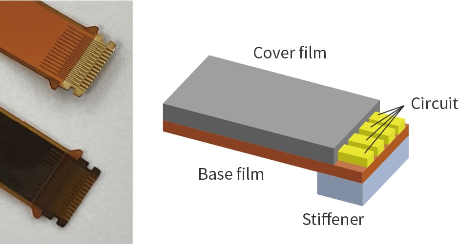
Structure of FPC
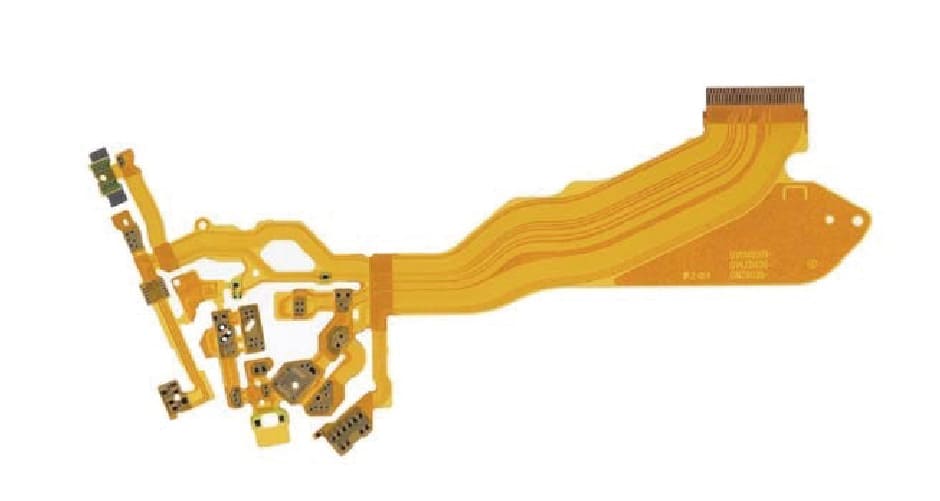
Single-sided FPC
Single-sided FPCs are thin, flexible, and highly bendable. Low springback helps to keep the shape of the FPC bent at the connecting area with a liquid crystal panel, and reduces power consumption for HDDs. Based on the details of your application and required performance, our experienced engineers will select the best materials for your purposes and provide FPCs with the appropriate characteristics to satisfy your requirements.
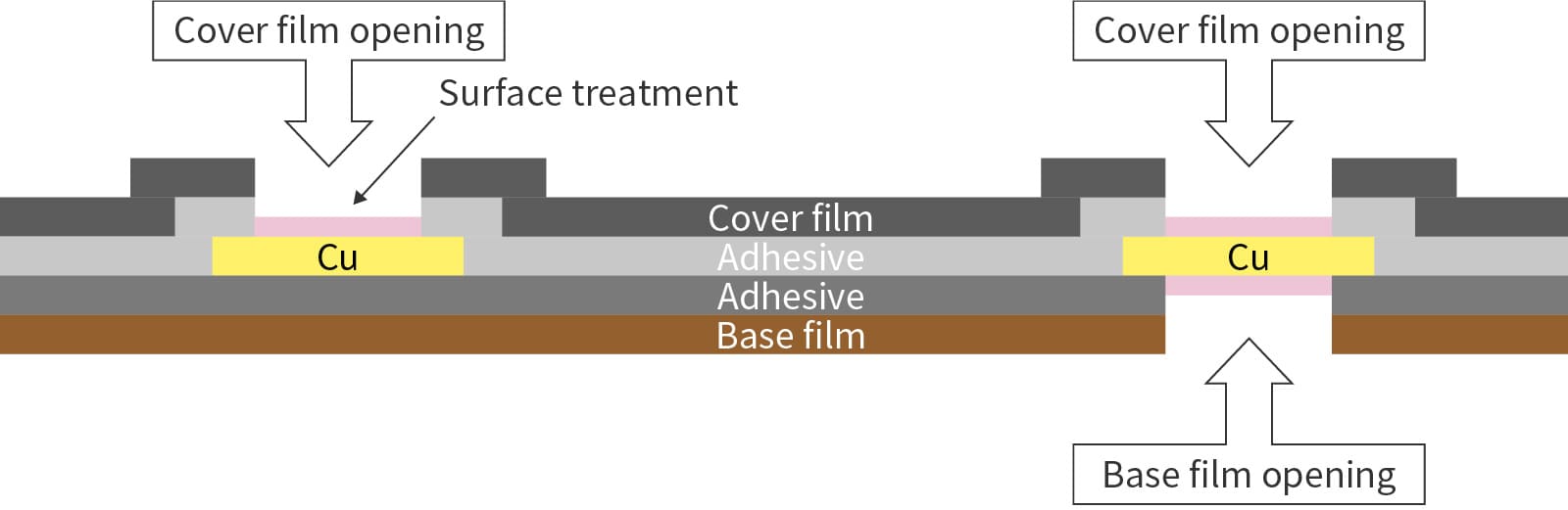
Structure
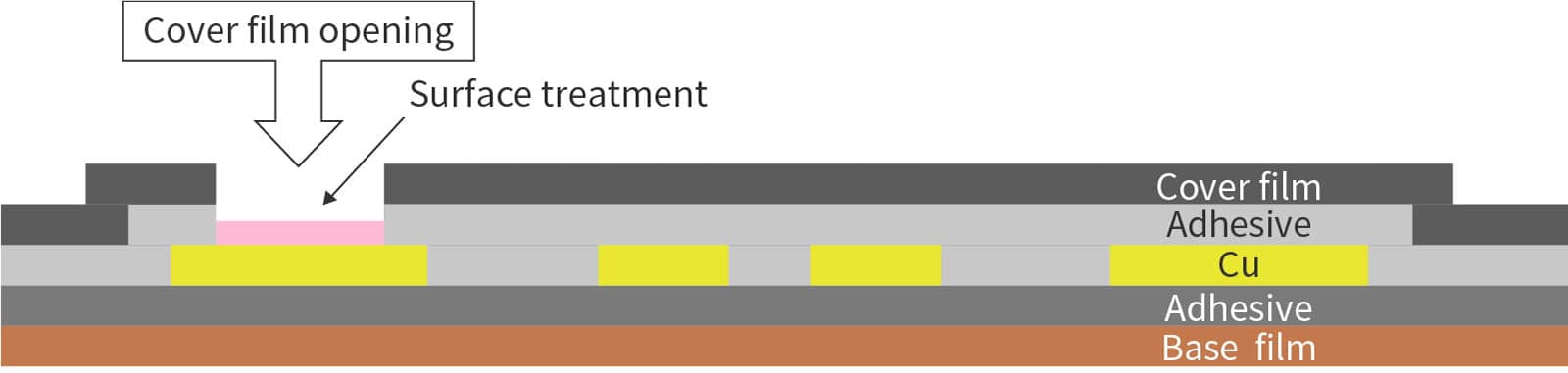
Standard design
| Structure name | Type | Thickness (µm) |
|---|---|---|
| Cover film | Polyimide | 12.5 , 25 |
| Cover film adhesive | Thermal curing | 15 , 20 , 25 , 30 , (50) |
| Copper foil | Rolled copper foil | 12 , 18 , 35 |
| Electrolytic copper foil | 12 , 18 , 35 , (70) | |
| Base film adhesive | Thermal curing | None , 10 |
| Base film | Polyimide | 12.5 , 25 |
| Surface treatment | Hard gold plating | Gold:0.03 or more / Nickel base:3〜9 |
| Soft gold plating | Gold:0.03 or more / Nickel base:3〜9 | |
| Electroless gold plating | Gold:0.03 or more / Nickel base:2〜6 | |
| OSP | ー |
| Item | Standard design | Remarks |
|---|---|---|
| Minimum circuit width | 35µm | With copper foil thickness: 12 µm |
| 50µm | With copper foil thickness: 18 µm | |
| 100µm | With copper foil thickness: 35 µm | |
| Minimum circuit space | 35µm | With copper foil thickness: 12 µm |
| 50µm | With copper foil thickness: 18 µm | |
| 100µm | With copper foil thickness: 35 µm | |
| FPC outline shape to outer circuit | 0.25 mm or more | ー |
| Cover film minimum opening | 0.7mm | ー |
| FPC outline shape to cover film opening | 0.5 mm or more | ー |
Applications
Single-sided FPCs are generally used in small spaces or electronic devices that require high bending strength.
- Electrical wiring in smartphones, mobile phones, digital cameras, video cameras, tablets, laptop PCs, etc.
- Liquid crystal display panel applications
- Applications that require high bending strength (printers, HDDs, optical-pickup devices, etc.)
Specifications
- Fine circuit
- Low springback force
- High bending durability
- Electrical noise shield
- Environmentally friendly (halogen-free)
- Flame resistant (UL standard compliant)
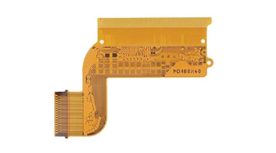
Double-sided FPC
Double-sided FPCs are generally inferior to single-sided FPCs in thickness, flexibility, and bending strength, but with optimal selection of materials and structures, they can provide characteristics similar to single-sided FPCs.
Double-sided FPCs allow high-density wiring and high-density component mounting.
Double-sided FPCs can control impedance for high-speed signal transmission.
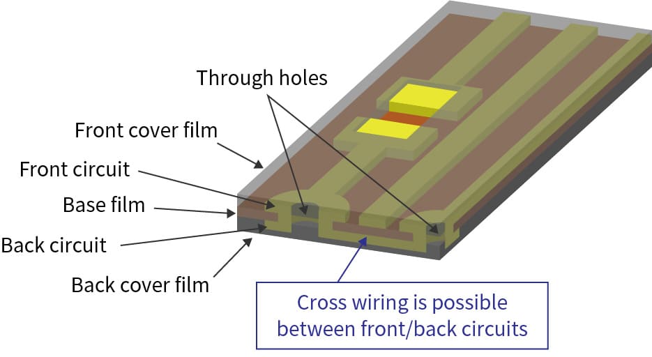
Structure
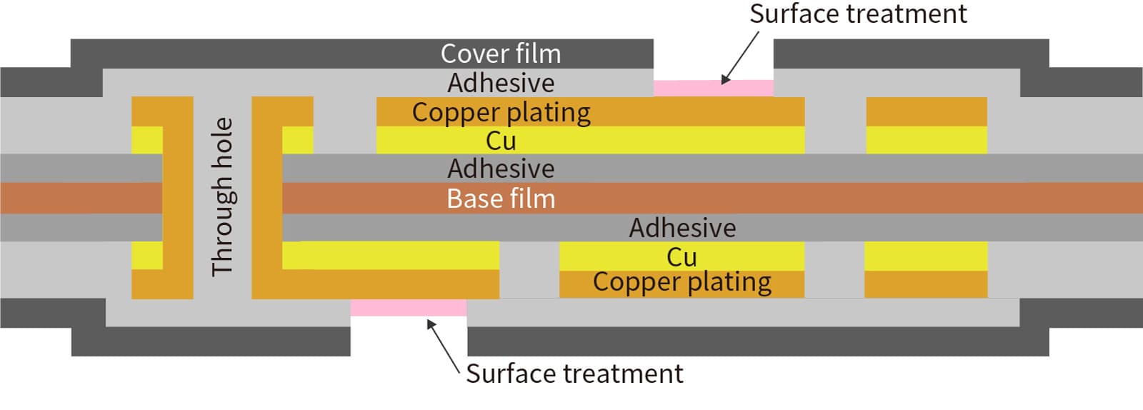
1.Through-hole connection
2.Via connection
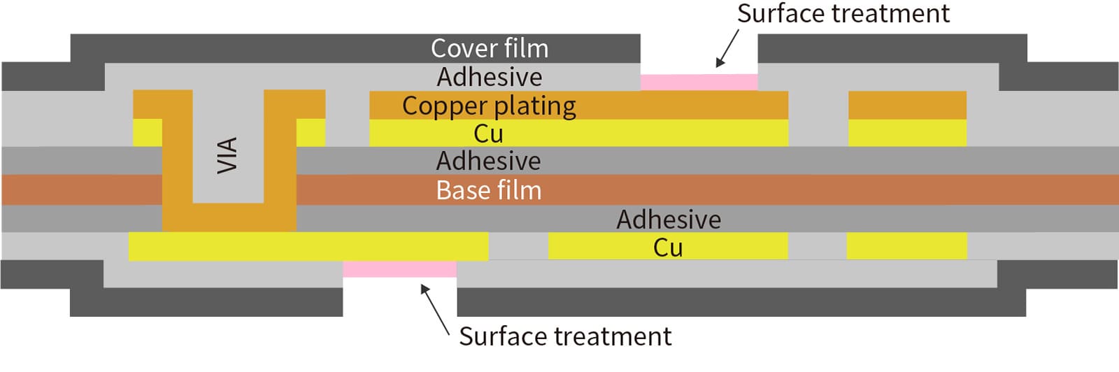
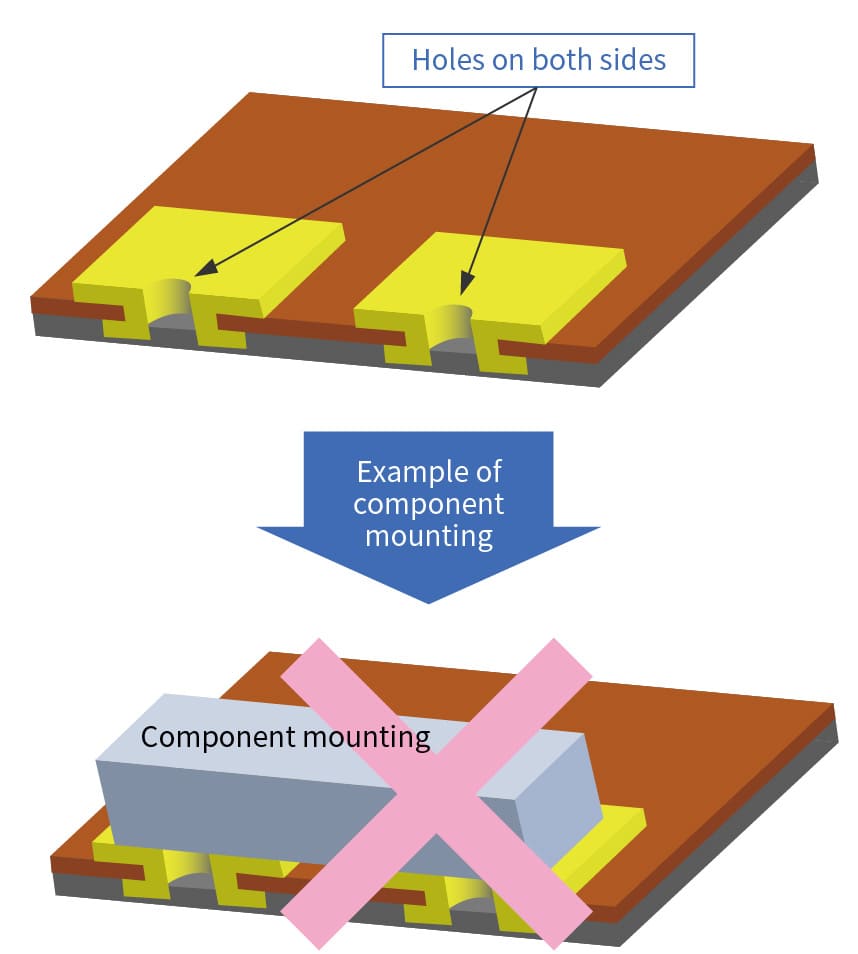
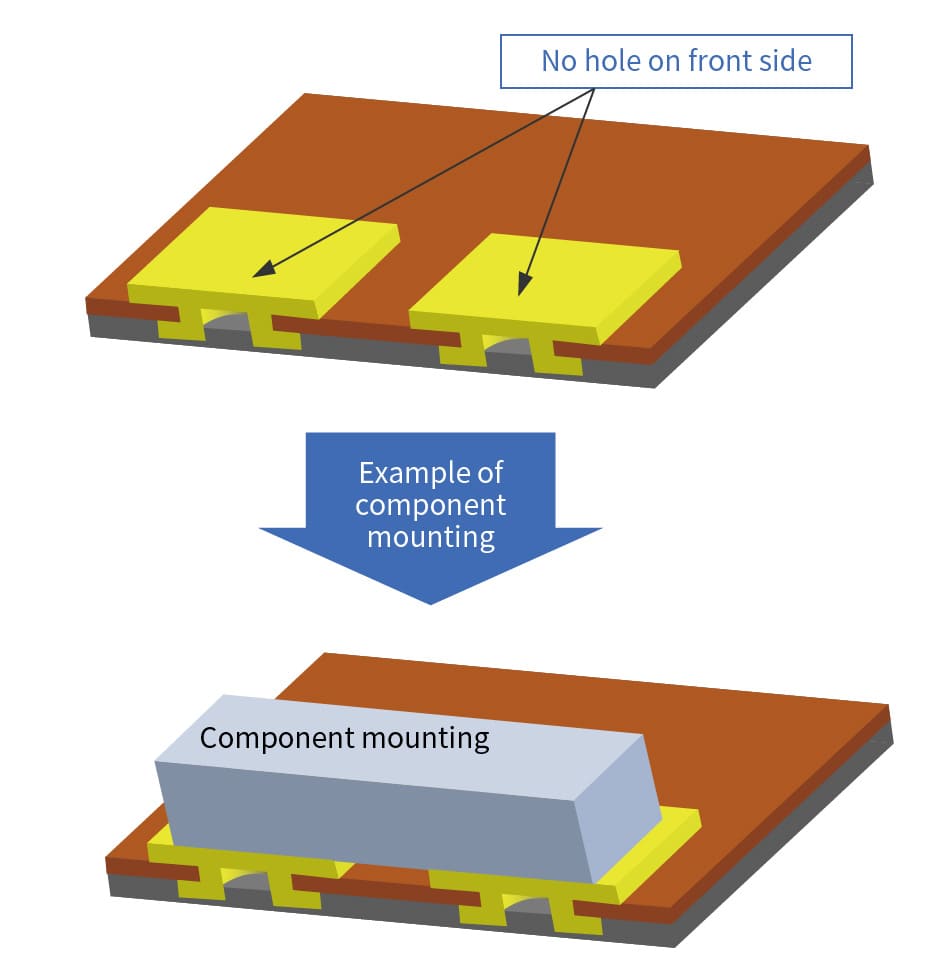
A through-hole connection has holes on both sides of the connecting area, while a via connection only has holes on one side.
With a “via connection” structure, via holes on the back side mean that the front side can be used as a contact pad or component mounting pad, allowing for even higher density mounting.
Standard design
| Structure name | Type | Thickness (µm) |
|---|---|---|
| Cover film | Polyimide | 12.5 , 25 |
| Cover film adhesive | Thermal curing | 20 , 25 , 30 |
| Copper foil | Rolled copper foil | 12 , 18 |
| Electrolytic copper foil | 12 , 18 | |
| Base film adhesive | Thermal curing | none , 10 |
| Base film | Polyimide | 12.5 , 25 |
| Copper plated on reverse side | ー | Select “None” for via |
| Surface treatment | Hard gold plating | Gold:0.03 or more / Nickel base:3〜9 |
| Soft gold plating | Gold:0.03 or more / Nickel base:3〜9 | |
| Electroless gold plating | Gold:0.03 or more / Nickel base:2〜6 | |
| OSP | ー |
| Item | Standard design | Remarks |
|---|---|---|
| Minimum circuit width | 50µm | With copper foil thickness: 12 µm + copper plated |
| 75µm | With copper foil thickness: 18 µm + copper plated | |
| 40µm | With copper foil thickness: 12 µm, via connection, copper plated on reverse side | |
| 50µm | With copper foil thickness: 18 µm, via connection, copper plated on reverse side | |
| Minimum circuit space | 50µm | With copper foil thickness: 12 µm + copper plated |
| 75µm | With copper foil thickness: 18 µm + copper plated | |
| 40µm | With copper foil thickness: 12 µm, via connection, copper plated on reverse side | |
| 50µm | With copper foil thickness: 18 µm, via connection, copper plated on reverse side | |
| Through hole diameter | 120 µm or higher | ー |
| Through hole land diameter | 300 µm or higher | Through hole diameter |
| Via diameter | 75 µm or higher | ー |
| Via land diameter | 275 µm or higher, Via diameter | +200 µm or higher |
| FPC outline shape to outer circuit | 0.25 mm or more | ー |
| Cover film minimum opening | 0.7mm | ー |
| FPC outline shape to cover film opening | 0.5 mm or more | ー |
Also available with “button plating” specification, where copper plating is only applied to the through-hole or via area. This allows thinner and more consistent copper thickness, while maintaining conductivity between the circuits on each side, which can improve circuit width accuracy and flexibility.
*Please contact us about items not listed above or special designs.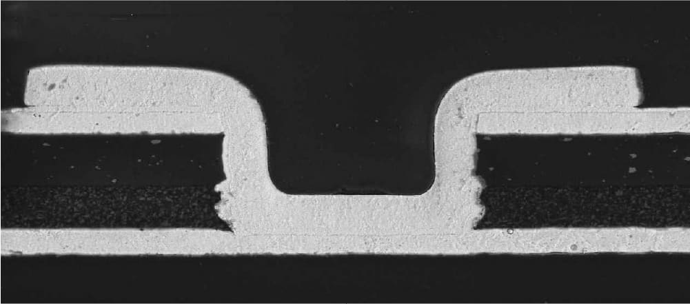
Applications
Double-sided FPCs are used in electronic components for high-density wiring that is not possible with single-sided FPCs.
- Electrical wiring in smartphones, mobile phones, digital cameras, video cameras, tablets, laptop PCs, etc.
- Liquid crystal display panel applications
- Applications that require high bendingdurability (HDDs, optical-pickup devices)
Specifications
- Fine circuit
- Low springback force
- Micro size via hole (LVH: laser via hole)
- High bending durability
- Electrical noise shield
- High-speed signal transmission (Impedance control)
- Environmentally friendly (halogen-free)
- Flame resistant (UL standard compliant) etc.
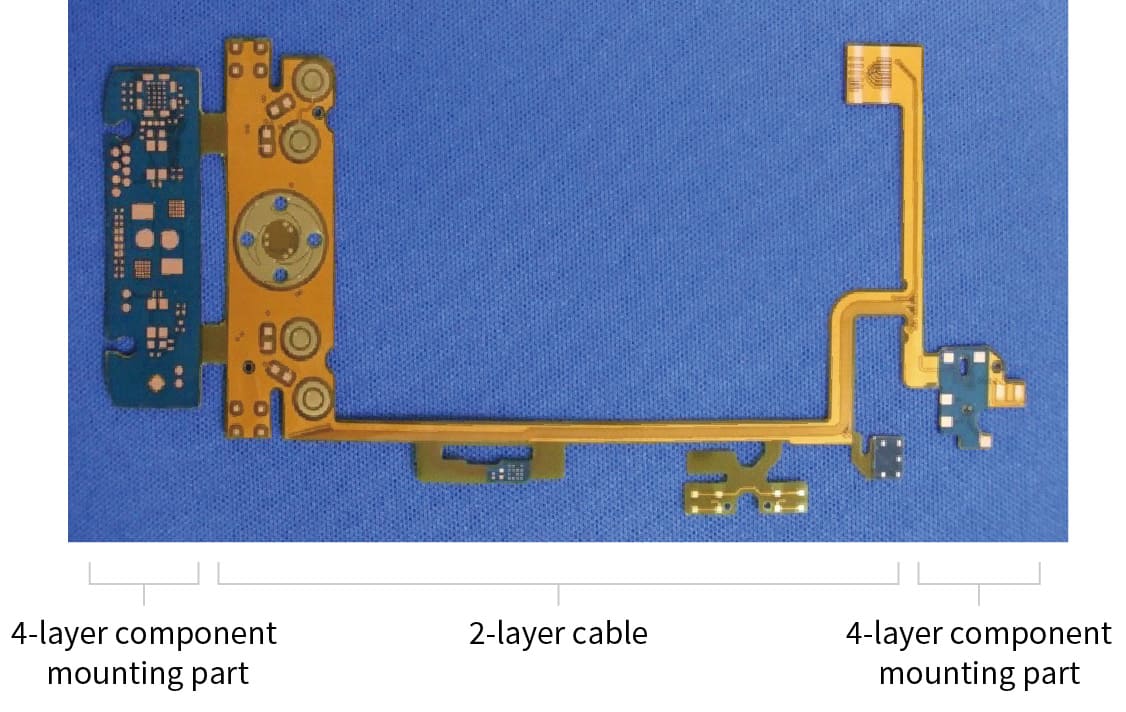
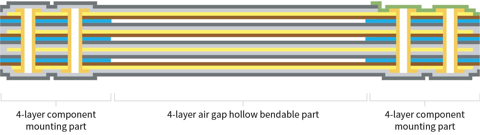
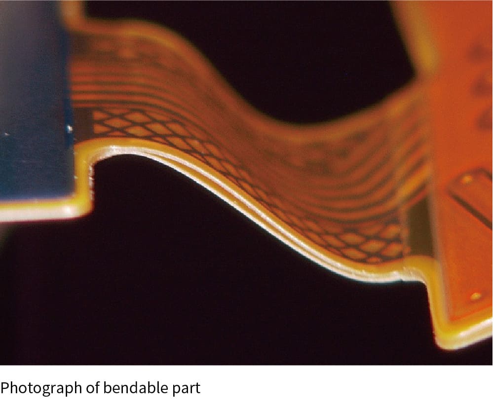
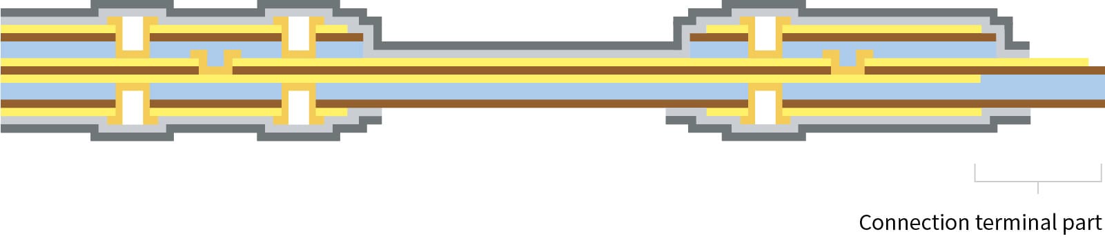
Multilayer FPC
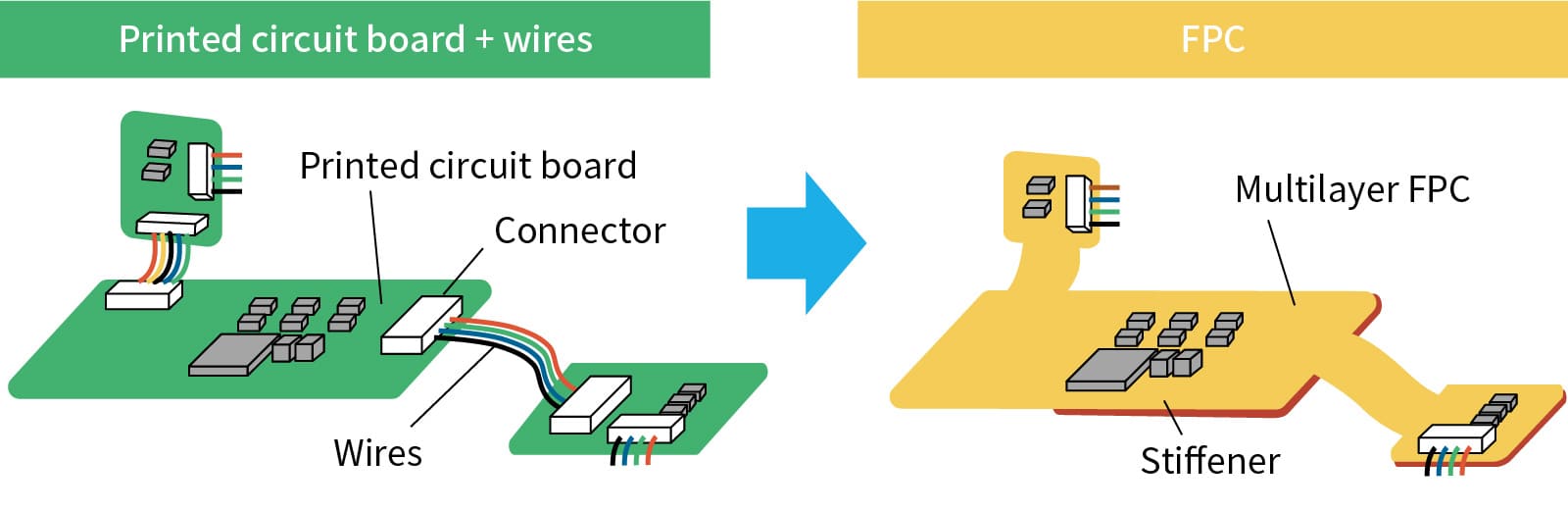
FPC with three or more layers of conductors. Rigid multilayer portions mounted with components and highly bendable lead portions are integrated in FPC. To effectively harness the characteristics of the FPC, a partially multilayered (laminated) structure is often used. We can supply FPCs incorporating various requirements. As the board and cables are integrated, there is no need for coupling parts like connectors, which saves space and offers high reliability.
Structure
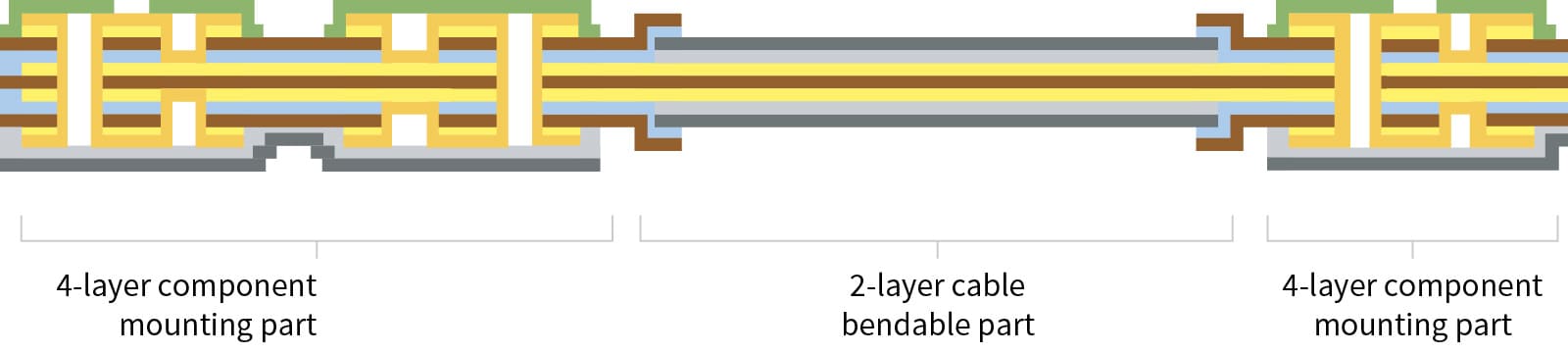
1.Partial multilayer
In this example, the bendable part has a two-layer structure and the component mounting part has a four-layer structure.
2.Air gap hollow structure
There is no adhesive between the layers in the bendable part, making this structure more bendable.
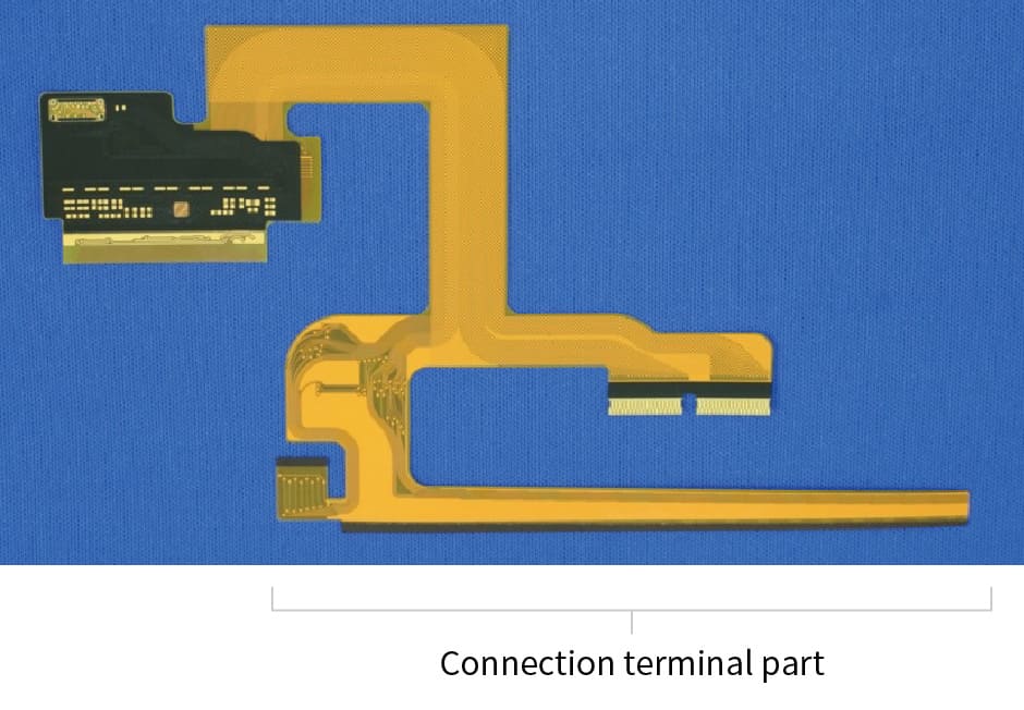
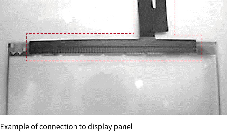
3.Flying tail
The connection terminal part has a single layer structure and uses ACF (Anisotropic Conductive Film) bonding, making it suitable for connection to display panels.
Standard design
| Structure name | Type | Thickness (µm) |
|---|---|---|
| Cover film | Polyimide | 12.5 , 25 |
| Cover film adhesive | Thermal curing | 20 , 25 , 30 |
| Copper plating | ー | 10 , 15 , 20 |
| Copper foil | Rolled copper foil | 12 , 18 |
| Electrolytic copper foil | 12 , 18 | |
| Base film adhesive | Thermal curing | none , 10 |
| Base film | Polyimide | 12.5 , 25 |
| Surface treatment | Hard gold plating | Gold:0.03 or more / Nickel base:3〜9 |
| Soft gold plating | Gold:0.03 or more / Nickel base:3〜9 | |
| Electroless gold plating | Gold:0.03 or more / Nickel base:2〜6 | |
| OSP | ー |
| Item | Standard design | Remarks |
|---|---|---|
| Minimum circuit width | 50µm | With copper foil thickness: 12 µm + copper plated |
| 75µm | With copper foil thickness: 18 µm + copper plated | |
| 40µm | With copper foil thickness: 12 µm, via connection, copper plated on reverse side | |
| 50µm | With copper foil thickness: 18 µm, via connection, copper plated on reverse side | |
| Minimum circuit space | 50µm | With copper foil thickness: 12 µm + copper plated |
| 75µm | With copper foil thickness: 18 µm + copper plated | |
| 40µm | With copper foil thickness: 12 µm, non copper plated layer | |
| 50µm | With copper foil thickness: 18 µm, non copper plated layer | |
| Through hole diameter | 120 µm or higher | ー |
| Through hole land diameter | 300 µm or larger | Through hole diameter+180 µm or larger |
| Via diameter | 75 µm or larger | ー |
| Via land diameter | 275 µm or higher | Via diameter: +200 µm or larger |
| Width between FPC outer shape and outer circuit | 0.25 mm or more | ー |
| Cover film minimum opening | 0.7mm | ー |
| FPC outer shape to cover film opening | 0.5 mm or more | ー |
Please contact us if you are interested in multilayer FPCs.
Applications
Multilayer FPCs are thin, flexible, and light, so they are used to create small, lightweight and well-designed electronic components.
- Electrical wiring in smartphones and tablets
- Camera modules, etc.
- Small electronic medical equipment and wearable devices, etc.
Specifications
- Fine circuit
- Low springback force
- Small via connection (through hole, BVH, IVH)
- Board-to-board interconnection
- High bending durability
- Electrical noise shield
- High-speed signal transmission (impedance control)
- Environmentally friendly (halogen-free)
- Flame resistant (UL standard compliant) etc.
Double side access FPC
This structure has a single conductor layer, with the base film partially removed so that the conductor layer is exposed on both sides. Whereas a normal single-sided FPC only allows electrical contact from the front side, a double side access FPC allows contact from both sides. In addition to the thin, flexible features of a single-sided FPC, this provides freedom to contact the conductive layer from both sides.
Structure
Standard design
| Structure name | Type | Thickness (µm) |
|---|---|---|
| Cover film | Polyimide | 12.5 , 25 |
| Cover film adhesive | Thermal curing | 20 , 25 , 30 , (50) |
| Copper foil | Rolled copper foil | (18) , 35 , (70) |
| Electrolytic copper foil | (18) , 35 | |
| Base film adhesive | Thermal curing | 20 , 25 |
| Base film | Polyimide | 25 |
| Surface treatment | Hard gold plating | Gold:0.03 or more / Nickel base:3〜9 |
| Soft gold plating | Gold:0.03 or more / Nickel base:3〜9 | |
| Electroless gold plating | Gold:0.03 or more / Nickel base:2〜6 | |
| OSP | ー |
Applications
Double side access FPCs are used in electronic components for high-density wiring that is not possible with single-sided FPCs.
- Industrial equipment
- Compact equipment
Specifications
- Low springback force
- High bending durability
- Electrical noise shield
- Environmentally friendly (halogen-free)